Concevez votre module LED à la carte.
Vos prototypes de modules LED en quelques clics
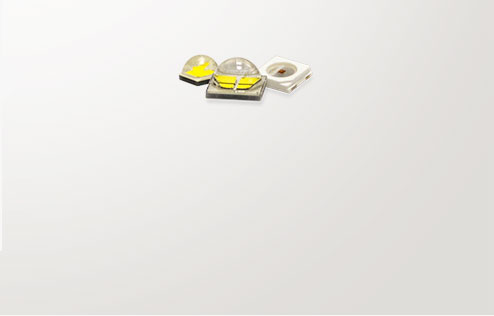
- Un large choix avec plus de 15 000 références
- Vos cartes reçues en 24h
- Vos prototypes avec le meilleur ratio prix/performance
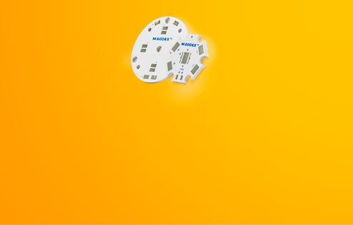
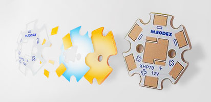
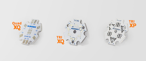
Le plus grand catalogue de MCPCB standards pour LED au Monde


Vos prototypes de modules LED en quelques clics